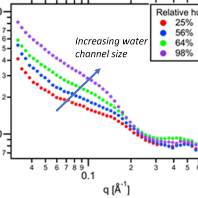
LLNL researchers have developed a method to enhance the performance of polyelectrolyte membranes by using a humidity-controlled crosslinking process which can be applied to precisely adjust the water channels of the membrane.
Image

A thyristor will stay conducting until the current through the device is zero (“current zero”) or perhaps slightly negative. LLNL’s approach is to use the opticondistor (“OTV”) to force this current zero in order to force the device into an “off” state. By combining a light-activated thyristor with an OTV, a noise-immune, high efficiency, high-power switching device can be constructed. The…
Image

The researchers’ approach leverages the concept that dopants have high diffusivities in Ga2O3; the key lies in the selection of the appropriate dopant. This LLNL invention describes two device types that employ this design:
Image

Design and construction of a photoconductive switch requires a diamond photoconductor illuminated by light of a certain excitation wavelength.
Characteristics of the LLNL-developed switch are as follows:
Image

LLNL researchers have invented an ultrafast PCSS to drive a high-power laser diode with arbitrary pulse widths. These devices operate by supplying a high voltage (>10 kV) to one side of the switch. A short pulse of light illuminates the semiconductor, instantly turning it from highly resistive to highly conductive.
Image

LLNL’s novel approach is to use diamond substrates with the desired donor (nitrogen) and acceptor (boron) impurities. In order to optically activate these deep impurities, the invention requires at least one externally or internally integrated light source. The initial exposure to light can set up the desired conduction current, after which the light source could be turned off. Even with…
Image

Instead of producing individual DSRDs and bonding them, Tunnel DSRD's entire stack structure is grown epitaxially on a n- or p-type silicon wafer, resulting in a novel, “monolithic” stacked DSRD. A tunnel diode is essentially a diode with very highly doped p and n regions such that the reverse breakdown voltage is 200 meV or lower.
Image
CMI—a DOE Energy Innovation Hub—is a public/private partnership led by the Ames Laboratory that brings together the best and brightest research minds from universities, national laboratories (including LLNL), and the private sector to find innovative technology solutions to make better use of materials critical to the success of clean energy technologies as well as develop resilient and secure…
Image
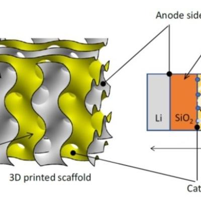
LLNL researchers have developed a new 3D printable lithium-air battery that uses a novel thin solid state ceramic electrolyte. LLNL’s invention overcomes the combined challenges of low power density and low cycle life in previously designed lithium-air batteries by using solid state electrolytes to achieve stability and multiscale structuring of the electrolyte to achieve low interfacial…
Image

U.S. Patent No. 11,555,965 describes LLNL’s invention of “Illumination Frustums” for photoconductive switches to capture and “frustrate” the light from leaving the frustum. LLNL researcher’s latest novel invention, “Twister Oven”, achieves this by encouraging laser light absorption in a photo conductor material. Light enters the oven twisting and reflecting, making near normal incident multi…
Image

For cooling a high power device, the novel approach is to use a thermoelectric cooler (TEC)-based embedded substrate with proper selection of the TEC material as an active cooler. The packaging configuration of TEC allows cooling the entire die without the use of a fluid. The process is compatible with the thin film TEC material. Standard semiconductor processes can be used to manufacture…
Image
Design and construction of a photoconductive switch requires a diamond photoconductor illuminated by light of a certain excitation wavelength. The diamond material is chosen to be doped with substitutional nitrogen to act as a source of electrons. The device architecture allows maximum light entering the aperture. The top and bottom electrodes are made of ultra-wide bandgap (UWBG)…
Image

LLNL researchers faced this challenge by bridging the gap between VEDs and solid-state electronics (SSE). Their approach was to create a hybrid vacuum microelectronic device (VMD) architecture that combines the properties of vacuum as the electronic medium and the compact form factor and manufacturing scalability of semiconductor microelectronic chips.
Image

For this method, a Silicon on Insulator (SOI) wafer is used to tailor etch rates and thickness in initial steps of the process. The simple three step process approach is comprised of grayscale lithography, deep reactive-ion etch (DRIE) and liftoff of the SOI wafer. The liftoff process is used to dissolve the insulating layer, thus separating sections of the wafer as individual silicon…
Image

The approach is to use Charge Balance Layers (CBLs) to create a superjunction device in wide bandgap materials. These CBLs enable the device to effectively spread the electric field over 2- or 3-dimensions within a semiconductor voltage sustaining layer instead of 1-dimension, thereby increasing the maximum voltage a device is capable of withstanding. The challenge of using CBLs is the…
Image

Design and construction of a photoconductive switch requires a diamond photoconductor illuminated by light of a certain excitation wavelength. The diamond material is specifically doped with substitutional nitrogen, which act as a source of electrons. The device architecture allows maximum light entering the aperture. The top and bottom electrodes are made of ultra wide band gap (UWBG)…
Image

The approach is to use a custom-designed frustrum and attach it to the optical fiber that connects to the PCSS. Light from the fiber enters the frustrum, spreads out, and enters the PCSS. Any unabsorbed light re-enters the frustrum and, because of its geometry, reflects back into the PCSS itself with only a negligible fraction escaping from the fiber. The shape of the novel frustrum is…
Image

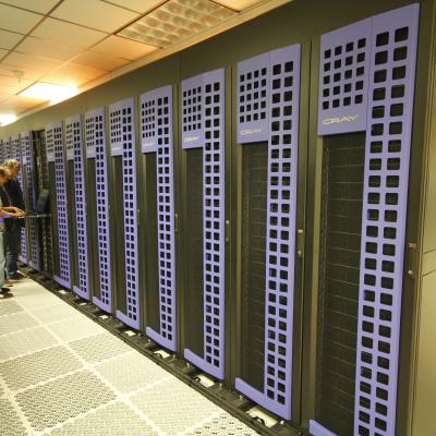
Lawrence Livermore National Laboratory (LLNL) is offering the opportunity to collaborate in accelerating artificial intelligence (AI) for applied science, including research in key areas such as advanced material design, 3D printing, predictive biology, energy systems, “self-driving” lasers and fusion energy research.
Image
Clinical images have a wealth of data that are currently untapped by physicians and machine learning (ML) methods alike. Most ML methods require more data than is available to sufficiently train them. In order to obtain all data contained in a clinical image, it is imperative to be able to utilize multimodal, or various types of, data such as tags or identifications, especially where spatial…
Image

Some COVID-19 diagnoses are utilizing computed tomography (CT)-scans for triage. CT-scans produce immediate results with high sensitivity. The digital images produced by a CT-scan require physicians to identify objects within the image to determine the presence of disease. Object identification can be done using machine learning (ML) techniques such as deep learning (DL) to improve speed and…
Image
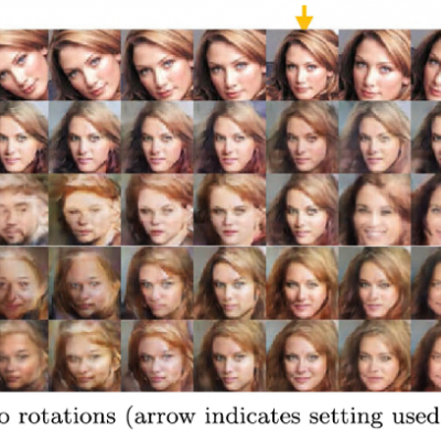
MimicGAN represents a new generation of methods that can “self-correct” for unseen corruptions in the data out in the field. This is particularly useful for systems that need to be deployed autonomously without needing constant intervention such as Automated Driver Assistance Systems. MimicGAN achieves this by treating every test sample as “corrupt” by default. The goal is to determine (a) the…
Image

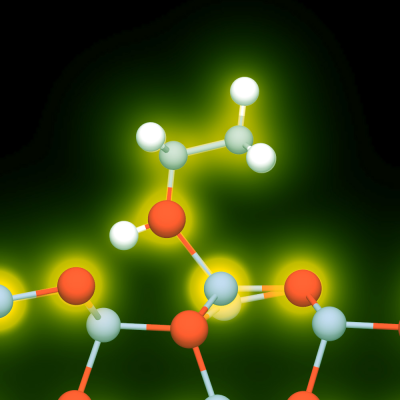
Livermore researchers have developed two novel TiCl4 based non-alkoxide sol-gel approaches for the synthesis of SiO2/TiO2 nanocomposite aerogels. Composite SiO2-TiO2 aerogels were obtained by epoxide-assisted gelation (EAG route) of TiCl4/DMF solution in the presence SiO2 aerogel particles. Additionally, the same TiCl4/DMF solution was employed to prepare SiO2@TiO2 aerogels by a facile one-…
Image
LLNL has developed a new system, called the Segmentation Ensembles System, that provides a simple and general way to fuse high-level and low-level information and leads to a substantial increase in overall performance of digital image analysis. LLNL researchers have demonstrated the effectiveness of the approach on applications ranging from automatic threat detection for airport security, to…
Image
Chemical and biological sensors based on nanowire or nanotube technologies exhibit observable ultrasensitive detection limits due to their unusually large surface-to-volume architecture. This suggests that nanosensors can provide a distinct advantage over conventional designs. This advantage is further enhanced when the nanosensor can harvest its meager power requirements from the surrounding…
Image

Nanomaterials that are emerging out of cutting edge nanotechnology research are a key component for an energy revolution. Carbon-based nanomaterials are ushering in the "new carbon age" with carbon nanotubes, nanoporous carbons, and graphene nanosheets that will prove necessary to provide sustainable energy applications that lessen our dependence on fossil fuels.
Carbon aerogels (CAs)…
Image
LLNL has developed novel nanoporous carbon materials for the surface-stress-induced actuator technology. The morphology of these materials has been designed to combine high surface area and mechanical strength. The process allows for the fabrication of large monolithic pieces with low densities and high structural integrity. One actuation technology relies on electrochemically- induced changes…