

LLNL developed a novel SOS diode structure starting with a n-type silicon wafer. On the appropriate sides of the wafer, donor and acceptor dopants with specifically designed and optimized concentration profiles are diffused in the structure. Crucially, an extra n-region is introduced to the structure to address pre-pulses. The result is a SOS diode with an optimized p+/p/n-…
Image

LLNL researchers have invented an ultrafast PCSS to drive a high-power laser diode with arbitrary pulse widths. These devices operate by supplying a high voltage (>10 kV) to one side of the switch. A short pulse of light illuminates the semiconductor, instantly turning it from highly resistive to highly conductive. Ultrawide bandgap (UWBG) semiconductors are used to achieve sub-…
Image

LLNL’s novel approach is to use diamond substrates with the desired donor (nitrogen) and acceptor (boron) impurities. In order to optically activate these deep impurities, the invention requires at least one externally or internally integrated light source. The initial exposure to light can set up the desired conduction current, after which the light source could be turned…
Image

Instead of producing individual DSRDs and bonding them, Tunnel DSRD's entire stack structure is grown epitaxially on a n- or p-type silicon wafer, resulting in a novel, “monolithic” stacked DSRD. A tunnel diode is essentially a diode with very highly doped p and n regions such that the reverse breakdown voltage is 200 meV or lower.
Image
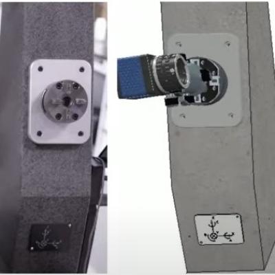
LLNL’s novel approach utilizes a number of techniques to improve reconstruction accuracy:
- Better coding scheme-based techniques
- Hardware-assisted techniques
- Adaptive fringe projection techniques
- Multi-exposure based techniques
The method requires specific calibration procedures and control of the hardware, which is achieved through a digital twin…
Image

For cooling a high power device, the novel approach is to use a thermoelectric cooler (TEC)-based embedded substrate with proper selection of the TEC material as an active cooler. The packaging configuration of TEC allows cooling the entire die without the use of a fluid. The process is compatible with the thin film TEC material. Standard semiconductor processes can be used…
Image

For this method, a Silicon on Insulator (SOI) wafer is used to tailor etch rates and thickness in initial steps of the process. The simple three step process approach is comprised of grayscale lithography, deep reactive-ion etch (DRIE) and liftoff of the SOI wafer. The liftoff process is used to dissolve the insulating layer, thus separating sections of the wafer as individual…
Image

The approach is to use Charge Balance Layers (CBLs) to create a superjunction device in wide bandgap materials. These CBLs enable the device to effectively spread the electric field over 2- or 3-dimensions within a semiconductor voltage sustaining layer instead of 1-dimension, thereby increasing the maximum voltage a device is capable of withstanding. The challenge of using CBLs is…
Image
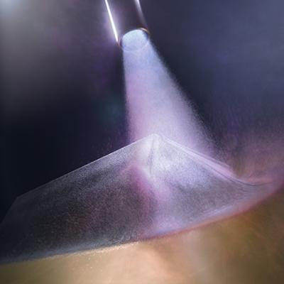
Versatile Cold Spray (VCS) enables deposition of brittle materials, such as thermoelectrics, magnets, and insulators, while retaining their functional properties. Materials can be deposited on substrates or arbitrary shapes with no requirement to match compositions. The VCS system is low cost, easily portable, and easy to use.
VCS has been developed in a collaboration between Lawrence Livermore…