
LLNL researchers have developed a method to of crosslinking, polymerizing or otherwise covalently coupling a subset of nitroaromatic and nitramine explosive molecules and compositions. Energetic materials manufactured using the novel method can be used ‘neat’ or as an energetic binder phase for another unmodified energetic compound. The approach may also be employed to co-…
Image

LLNL developed a novel SOS diode structure starting with a n-type silicon wafer. On the appropriate sides of the wafer, donor and acceptor dopants with specifically designed and optimized concentration profiles are diffused in the structure. Crucially, an extra n-region is introduced to the structure to address pre-pulses. The result is a SOS diode with an optimized p+/p/n-…
Image

LLNL researchers have developed an approach to form silicon carbide (and diamond) nanoneedles using plasma etching that create micro pillars followed by chemical etching of the pillars in forming gas containing hydrogen and nitrogen. Combining these two etching processes allow for fabrication of micro- and nanoneedles that are thinner and sharper than conventionally fabricated needles.
Image
LLNL has developed a method that adds a polyamine based crosslinker and an acid receptor, based on MgO nanoparticles into a polymer bonded PBX, where the polymer binder is a fluoropolymer containing vinylidene difluoride functionality. Crosslinking kinetics can then be controlled by selecting an appropriate amine structure, pressing temperature and optionally the addition of a chemical…
Image

LLNL researchers have designed and developed a novel high-density, high-channel count 3D connector that enables hundreds or thousands of nonpermanent connections within a compact footprint. The connector addresses limitations of currently used conventional approaches that were described previously, which have an artificial ceiling on the number of recording sites of modern devices of no more…
Image
LLNL researchers uses Additive Manufacturing (AM) to create reinforcing scaffolds that can be integrated with High Explosives (HE) or solid rocket fuel with minimal volume fraction. Its main benefit is to create stability in harsh field conditions. Its secondary benefit is providing another method to finely tune blast performance or fuel burn. Creating complex shapes with structural…
Image

LLNL researchers have invented an ultrafast PCSS to drive a high-power laser diode with arbitrary pulse widths. These devices operate by supplying a high voltage (>10 kV) to one side of the switch. A short pulse of light illuminates the semiconductor, instantly turning it from highly resistive to highly conductive. Ultrawide bandgap (UWBG) semiconductors are used to achieve sub-…
Image

LLNL’s novel approach is to use diamond substrates with the desired donor (nitrogen) and acceptor (boron) impurities. In order to optically activate these deep impurities, the invention requires at least one externally or internally integrated light source. The initial exposure to light can set up the desired conduction current, after which the light source could be turned…
Image

Instead of producing individual DSRDs and bonding them, Tunnel DSRD's entire stack structure is grown epitaxially on a n- or p-type silicon wafer, resulting in a novel, “monolithic” stacked DSRD. A tunnel diode is essentially a diode with very highly doped p and n regions such that the reverse breakdown voltage is 200 meV or lower.
Image

For cooling a high power device, the novel approach is to use a thermoelectric cooler (TEC)-based embedded substrate with proper selection of the TEC material as an active cooler. The packaging configuration of TEC allows cooling the entire die without the use of a fluid. The process is compatible with the thin film TEC material. Standard semiconductor processes can be used…
Image

For this method, a Silicon on Insulator (SOI) wafer is used to tailor etch rates and thickness in initial steps of the process. The simple three step process approach is comprised of grayscale lithography, deep reactive-ion etch (DRIE) and liftoff of the SOI wafer. The liftoff process is used to dissolve the insulating layer, thus separating sections of the wafer as individual…
Image

The approach is to use Charge Balance Layers (CBLs) to create a superjunction device in wide bandgap materials. These CBLs enable the device to effectively spread the electric field over 2- or 3-dimensions within a semiconductor voltage sustaining layer instead of 1-dimension, thereby increasing the maximum voltage a device is capable of withstanding. The challenge of using CBLs is…
Image
Many of the disadvantages of current interface devices can be overcome with LLNL’s novel interface design, which relies on area array distribution where independent interface connector subassemblies are positioned in a planar grid. Not only is the interface device expandable area-wise (without increasing contact force), but it could also be expanded height-wise, with multiple layers of…
Image
Commercial fiber optic cables are the current standard for carrying optical signals in industries like communications or medical devices. However, the fibers are made of glass, which do not have favorable characteristics for applications that require flexibility and re-routing, e.g. typically brittle, limited selection of materials, dimension constraints.
Image
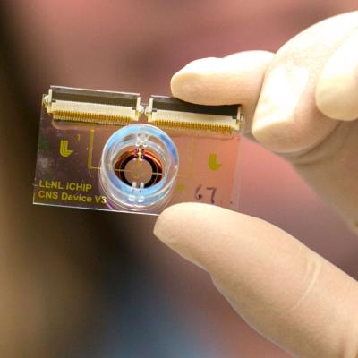
LLNL has developed a brain-on-a-chip system with a removable cell-seeding funnel to simultaneously localize neurons from various brain regions in an anatomically relevant manner and over specific electrode regions of a MEA. LLNL’s novel, removable cell seeding funnel uses a combination of 3D printing and microfabrication that allows neurons from select brain regions to easily be seeded into…