
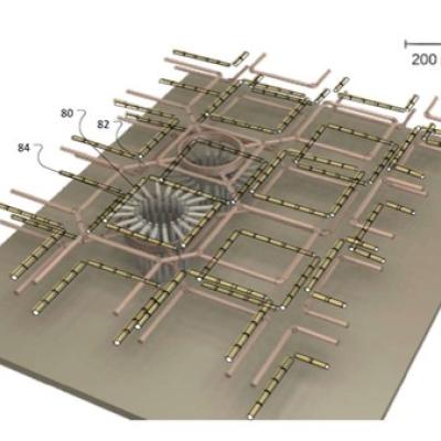
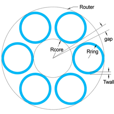
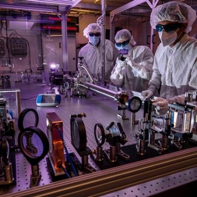
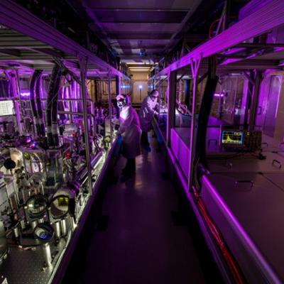
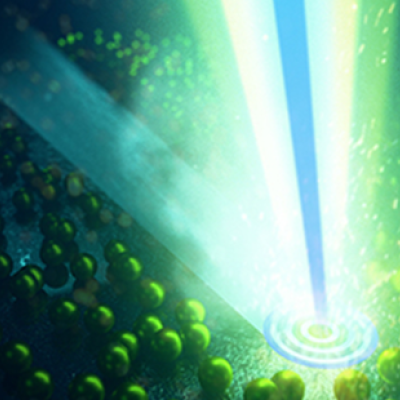
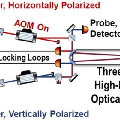
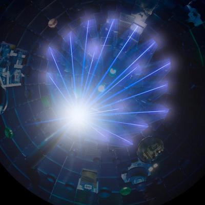
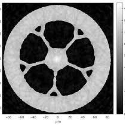
LLNL and its research partners have created miniature ion traps with submicron precision and complex geometries made using 3D printing for fast, high-fidelity and scalable quantum computations. A patent is pending on the technology, with claims covering embodiments for a vertical ion trap, horizontal ion traps and methods of forming the ion traps using advanced manufacturing techniques.
…Image
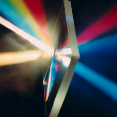
The approach is to use foundational materials science, structural design, thermal analysis, optic fabrication, and space systems engineering, and to use optimize them through large-scale simulation to realize meter-scale telescopes at 10X cost reduction. LLNL’s folded Gregorian design integrates all alignment sensitive components into one static monolithic system. Like solid-…
Image

LLNL developed a novel SOS diode structure starting with a n-type silicon wafer. On the appropriate sides of the wafer, donor and acceptor dopants with specifically designed and optimized concentration profiles are diffused in the structure. Crucially, an extra n-region is introduced to the structure to address pre-pulses. The result is a SOS diode with an optimized p+/p/n-…
Image

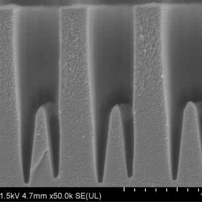
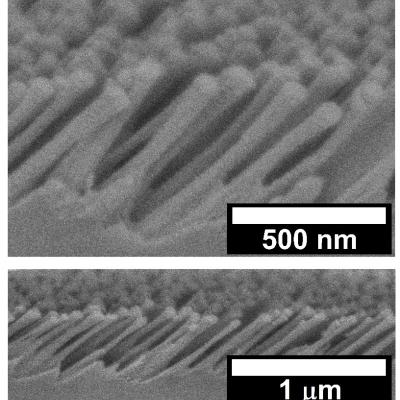
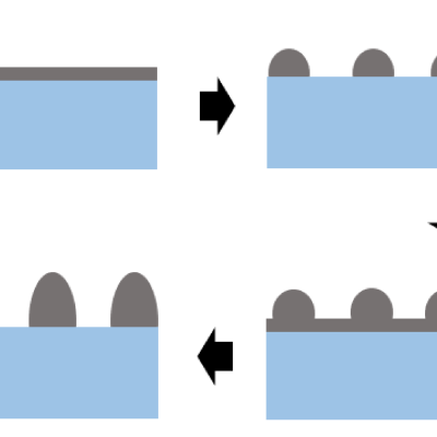
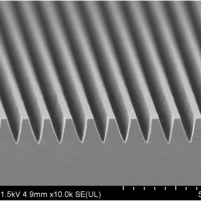
LLNL researchers have developed an approach to form silicon carbide (and diamond) nanoneedles using plasma etching that create micro pillars followed by chemical etching of the pillars in forming gas containing hydrogen and nitrogen. Combining these two etching processes allow for fabrication of micro- and nanoneedles that are thinner and sharper than conventionally fabricated needles.
Image

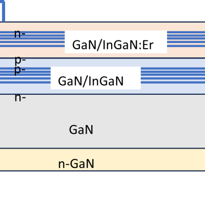
The approach is to use appropriately doped semi-insulating gallium nitride to provide a high damage tolerant photoconductor with high responsivity to various pump wavelength light. Mn, C, or Fe are used as dopants to provide a source of electrons or holes that can be excited. This is combined with the use of dichroic antireflection coating at the GaN/polyimide/liquid crystal…
Image

This LLNL invention introduces a technique for optimally detuning the ADC and signal clocks while maintaining synchronization between the two to manage correlated errors in waveform processing. This technique maintains synchronization between the two clocks, but with optimal detuning applied the interleaving artifacts are maximally decorrelated across waveforms and thus suppressed with…
Image
This LLNL invention allows for the fabrication of complex waveplate features and topologies from fused silica, a highly desirable and durable waveplate material. It also is a unique technique for density multiplication and high-fidelity bidirectional deposition, which can create optical components that are generally for entirely new classes of optical materials.
Left Image Caption…
Image
LLNL researchers have developed a relatively large electrochemically active window with low sheet resistance yet has dramatically increased RF transmission. In-situ measurements show an ~40% increase in reflection at 12GHz when tinting for 10 minutes as compared to the off state. The researchers achieved this through combining novel geometric design of the metal traces with the…
Image
This LLNL invention proposes a new microstructured large mode area fiber design that enhances the confinement of the core mode while strongly suppressing thermal or scattering mediated dynamic couplings with higher order modes thought to be responsible for generating undesirable Transverse Mode Instabilities. The design accomplishes higher order mode suppression and core mode confinement by…
Image
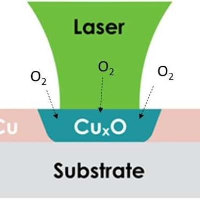
LLNL researchers developed a novel strategy that involves material transformations such as oxidation, nitridation, or carbonization. In one embodiment, copper is heated under ambient conditions resulting in its surface being oxidized and turned into copper oxide, where a new material (e.g., copper oxide) is developed via transformation (e.g., oxidation) without additional addition deposition…
Image
LLNL researchers have created a suitably compliant adhesive that is based on a thiol monomer mixed with an epoxy monomer in the presence of metal oxide nanoparticles. When cured into films or pucks, the adhesives are optically transparent with a RI up to ~1.68 at 532 nm with varying shore A hardness in the range of 50 to 98. The adhesive can potentially be mixed and potted between Ti:…
Image
LLNL researchers have continued to develop their pioneering DIW 3D-printed glass optics technology that allows for the 3D printing of single- and multi-material optical glass compositions in complex shapes. This LLNL invention further proposes incorporating dopants (including, but not limited to TiO2 and Pd) into slurries and inks for 3D printing of glass components that can then be directly…
Image
This LLNL invention is a wide bandgap (WBG) or ultra-wide bandgap (UWBG) material comprising a PCSS that is modified, either chemically through alloying and/or mechanically through strain fields, in order to tune the energetic positions of the valence and/or conduction bands and the associated optical transition energies that create and quench the PCSS responsivity.
Image
This LLNL invention concerns a method for patterning the index of refraction by fabricating a spatially invariant metasurface, and then apply spatially varied mechanical loading to compress the metasurface features vertically and spread them radially. In doing so, the index of refraction can be re-written on the metasurface, thus enabling index patterning. This process allows rapid 'rewriting…
Image

This invention proposes achieving the same effect of a single, high intensity pulse through the use of a closely spaced burst of short duration pulses. By keeping the intensity of the individual pulses below the damage threshold the risk of catastrophic damage is greatly mitigated. Additionally, the pulses are directed to strike the target at locations temporally and spatially sufficiently…
Image
LLNL’s Distributed Implicit Neural Representation (DINR) is a novel approach to 4D time-space reconstruction of dynamic objects. DINR is the first technology to enable 4D imaging of dynamic objects at sufficiently high spatial and temporal resolutions that are necessary for real world medical and industrial applications.
Image
Holography fully encodes a 3D light field by imprinting its interference pattern with a reference laser beam in a nonlinear medium. By crossing two pump laser pulses in a gas jet, a hologram can be recorded as a distribution of plasma, allowing manipulation of a subsequent high-intensity probe beam. The interference between two collinear beams with distinct foci produces a plasma zone plate, a…
Image
This invention proposes the use of a nonlinear spectral broadening subsystem as a post-CPA pulse compression add-on for high energy laser systems. The proposed solution utilizes the beam profile of a high peak power laser as a reference to shape a highly transmissive nonlinear plastic (e.g., CR39) itself to ensure a spatially homogeneous nonlinear spectral broadening.
Image

Powder atomic layer deposition process is used to coat nanopowders of host materials (e.g. yttrium aluminum garnet) with optically active neodymium organometal precursor followed by O2/O3 RF plasma to convert to a single layer of Nd2O3. The process can be repeated to build arbitrarily thick layers with custom doping profiles and followed by post-…
Image
This novel invention specifically enables the fabrication of arbitrarily tailored birefringence characteristics in nano-structured meta-surfaces on non-birefringent substrates (e.g. fused silica). The birefringent nano-structured meta-surface is produced by angled directional reactive ion beam etching through a nano-particle mask. This method enables the simultaneous tailoring of refractive…
Image
This invention (US Patent No. 11,294,103) is an extension of another LLNL invention, US Patent No. 10,612,145, which utilizes a thin sacrificial metal mask layer deposited on a dielectric substrate (e.g. fused silica) and subsequently nanostructured through a laser generated selective thermal de-wetting process.
Image
This invention proposes fabrication of a sandwich of two or more (typically 3) magneto-rheologically finished (MRF’d) birefringent plates with purpose designed arbitrary surface contour profiles and eigen-axis orientation. The tailored surface contour profiles are designed to compensate for the observed de-polarization characteristics of a particular solid-state laser operating in a particular…
Image

LLNL researchers have developed a TDLAS-based, standalone, real-time gas analyzer in a small form-factor for continuous or single-point monitoring. The system can analyze multiple gases with ultra-high sensitivity (ppm detection levels) in harsh conditions when utilizing wavelength-modulation spectroscopy (WMS).
Image
This LLNL invention is an optical amplifier, wherein the gain element is in the form of a frustum and a spherically diverging laser beam is introduced into the gain medium via the small face of the frustum. In one embodiment, the pump beam is generated by one or more chromium-lasers that are counter-propagating, having been introduced through the large face of the frustum. The gain medium may…
Image

This invention circumvents the GMAPD deadtime limitation by using an array of GMAPDs in a non-imaging configuration instead of a single element. By using an array, with sufficient number of elements, guarantees there is always at least one element available to detect an incoming photon even if others are in the deadtime zone.
Image
This invention works by imaging an ultrafast pulse diffracted from a large grating onto a spatial light modulator (SLM) thereby directly transcribing an arbitrary record on a pulse front tilted (PFT) ultrafast pulse. The grating generates PFT of the input pulse, and the SLM provides temporal control of the pulse through the space-to-time mapping of the tilted pulse. Coupling this patterned…
Image
The essence of this invention is a method that couples network architecture using neural implicit representations coupled with a novel parametric motion field to perform limited angle 4D-CT reconstruction of deforming scenes.
Image
This invention exploits the non-linearities of optical Mach-Zehnder (MZ) electrooptic modulators to enhance small signal dynamic range at higher bandwidths. A linear photodiode (PD) converts the amplified optical signal output from the MZ back to an electrical signal completing an Electrical-Optical-Electrical (EOE) conversion cycle. The dynamic range can be further enhanced by daisy chaining…
Image
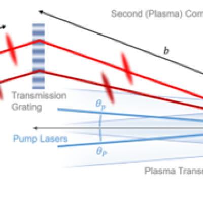
This invention draws on the higher damage tolerance of plasma to manipulate high-intensity light. Plasma is a difficult medium to control and sets stringent limits on optical performance. A compact high-power laser system can be realized using plasma transmission gratings for chirped pulse compression based on currently achievable plasma properties and minimal plasma volume. A double…
Image
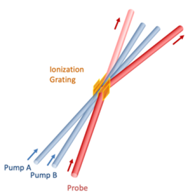
This invention proposes a volumetric transmission grating based on ionization created in a neutral gas by crossing and interfering two short-pulse pump lasers so that their intensity maxima rise above the medium’s ionization threshold. This will create a modulated index of refraction that can diffract a subsequent probe beam like a transmission grating. Crucially for the application of…
Image

A thyristor will stay conducting until the current through the device is zero (“current zero”) or perhaps slightly negative. LLNL’s approach is to use the opticondistor (“OTV”) to force this current zero in order to force the device into an “off” state. By combining a light-activated thyristor with an OTV, a noise-immune, high efficiency, high-power switching device can be…
Image

The researchers’ approach leverages the concept that dopants have high diffusivities in Ga2O3; the key lies in the selection of the appropriate dopant. This LLNL invention describes two device types that employ this design:
Image

This invention proposes using a pulse laser configured to generate laser pulses and a controller for controlling operation of the pulse laser. The controller is further configured to control the pulse laser to cause the pulse laser to generate at least one of the laser pulses with a spatiotemporally varying laser fluence over a duration of at least one of the laser pulses. The spatiotemporally…
Image
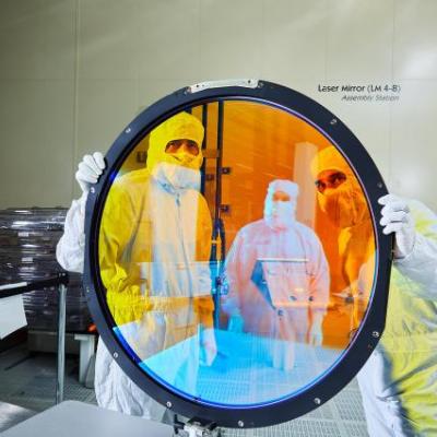
Rapid monolith development at scale is achieved through use of a functionally equivalent optic simulant made from a low-cost material to substitute the functional optic. Monolith optical performance is affected not only by thermal expansion but also by temperature inhomogeneity due to the temperature dependence of refractive index.
Image
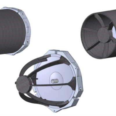
Aeroptics are a proposed new class of monolithic optical system in aerogel fabricated by molding around a master mandrel. This approach combines the intrinsic stability of proven monolithic telescopes, with the ultralow density of silica aerogels. In Aeroptics, the monolith is hollow with an aerogel substrate providing a supporting structure. Theoretically, Aeroptics could enable 1-m aperture…
Image

This invention proposes to engineer the current density along the length of a laser diode to overcome the penalty associated with non-uniformity resulting from asymmetry in the gain, photon or carrier density despite having uniform contact. Optimizing the current density profile enables diode lasers to operate with greater power conversion efficiency or operate with equivalent power conversion…
Image

This invention proposes to engineer the temperature dependence of the emission wavelength of LEDs and laser diodes. The approach is to use a strain-inducing coating to counteract the intrinsic temperature coefficient of the emission wavelength of the LED or laser diode device thereby rendering it athermal. This invention avoids additional complexity, size, weight and power dissipation of…
Image

This invention proposes a method to overcome the key limitation of electrically pumped lasers based on AlN, AlGaN, or AlInGaN, namely the lack of suitable shallow donor and acceptor dopants. As the band gap of these materials increases (and the emission wavelength decreases), both electrons and holes require greater thermal energies in order to ionize.
Image
Laser diode lensing effect can be substantially reduced by creating a pattern interface such that the substrate is only attached at the diode mesa. This is achieved by either creating a pattern solder joint and/or pattern substrate.
Image

Design and construction of a photoconductive switch requires a diamond photoconductor illuminated by light of a certain excitation wavelength.
Characteristics of the LLNL-developed switch are as follows:
Image

LLNL researchers has developed designs to augment WBG/UWBG-based OALVs to improve their power handling capability under CW operational environments. These designs include:
Image
This invention takes advantage of the high water-solubility of key NIF KDP crystal optics and uses water as an etchant to remove surface defects and improve the laser induced damage threshold. Since pure water etches KDP too fast, this invention is to disperse water as nanosized droplets in a water-in-oil micro-emulsion. While in a stable micro-emulsion form, the surfactant additives prevent…
Image
This invention proposes to use laser induced melting/softening to locally reshape the form of a glass optic. The local glass densification that results induces predictable stresses that through plate deformation mechanics yield a deterministic methodology for arbitrarily reshaping an optic surface figure and wavefront without the need to remove material.
Image
This invention achieves both a wider field of view and faster f-number within a monolithic substrate by incorporating an aspheric convex refractive first surface and a planar aspheric field corrector surface on the final refractive surface. These two refractive surfaces work in conjunction with a concave aspheric primary and convex aspheric secondary mirror (e.g. Cassegrain type) to improve…
Image

This invention is about a Material Jetting technique used to form a ceramic green body that is subsequently processed into a transparent ceramic optic with unique tunable spatial control of the composition as a function of position only achievable via additive manufacturing methods. This method uses ceramic particles loaded into a liquid slurry with required viscosity and surface tension to be…
Image
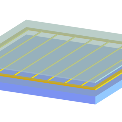
This invention consists of a method of forming nanoscale metal lines to produce a grating-like mask with wide area coverage over the surface of a durable optical material such as fused silica. Subsequent etching processes transfer the metal mask to the underlying substrate forming a birefringent metasurface. This method enables the production of ultrathin waveplates for high power laser…
Image
This LLNL invention proposes a novel approach to spectral interferometry, the preferred technique for characterizing nanosecond long records of laser pulse shapes with femtosecond resolution. Linear techniques are much more sensitive than the many nonlinear techniques of the prior art and can be used for very weak pulses. However, they depend on being able to interfere the signal with a well…
Image
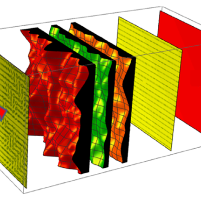
LLNL has designed and demonstrated a novel transmission Spectral Beam Combining grating optic assembly with megawatt power handling capabilities. The design consists of a monolithic structure with an input transform optic and an output transmission grating. The design features LLNL’s proven compact, lightweight Spectral Channels Splicer architecture to combine adjacent spectral channels of…
Image
Heat sensitive materials such as piezoelectric and MEMS devices and assemblies, magnetic sensors, nonlinear optical crystals, laser glass or solid-state laser materials, etc. cannot be exposed to excess temperatures which in the context of this invention, means materials that cannot be exposed to temperatures greater than 50°C (122°F). LLNL’s invention describes a low-temperature method of…
Image

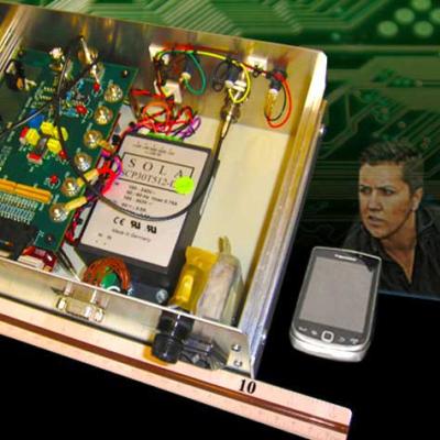
LLNL researchers have developed a novel Radio Frequency Identification (RFID), tracking, powering system and method using coded Ultra-wideband (UWB) signaling. The RFID system is capable of remote powering (activating) multiple passive UWB tags that are located some distance away, which is further than conventional RFID tags. Once the tags are activated, the tags are able to communicate with…
Image

LLNL researchers have invented an ultrafast PCSS to drive a high-power laser diode with arbitrary pulse widths. These devices operate by supplying a high voltage (>10 kV) to one side of the switch. A short pulse of light illuminates the semiconductor, instantly turning it from highly resistive to highly conductive. Ultrawide bandgap (UWBG) semiconductors are used to achieve sub-…
Image
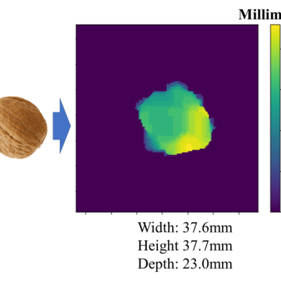
LLNL’s novel technology automates the inspection process by using a scanning system that captures data within the walnut shell without having to open the shell. The system output gives a visual image inside the walnut shell sufficient to evaluate and rate the quality of the walnut. The system uses a camara and radar that can capture data at a rapid rate. This improves speed and…
Image
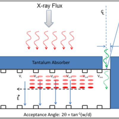
The approach is to develop a solid-state X-ray imager based on the architecture of the Silicon Drift Detector (SDD) which uses a series of cathode strips on both sides of a silicon wafer to achieve bulk depletion and electron drift. The invention leverages this SDD functionality to achieve signal stretching of liberated charge carriers from X-Ray photons that converts the time domain…
Image

The approach is to leverage the fact that a momentary “load” equal to the power transmission line impedance, (Z0), during the transient can suppress its propagation. Z(0) is typically a fixed impedance of several hundred ohms based on the geometry of most single wire transmission lines.
So, an isolated self-powered opticondistor (OTV) system may provide an ultrafast method of…
Image

LLNL’s novel approach is to use diamond substrates with the desired donor (nitrogen) and acceptor (boron) impurities. In order to optically activate these deep impurities, the invention requires at least one externally or internally integrated light source. The initial exposure to light can set up the desired conduction current, after which the light source could be turned…
Image

Instead of producing individual DSRDs and bonding them, Tunnel DSRD's entire stack structure is grown epitaxially on a n- or p-type silicon wafer, resulting in a novel, “monolithic” stacked DSRD. A tunnel diode is essentially a diode with very highly doped p and n regions such that the reverse breakdown voltage is 200 meV or lower.
Image
LLNL researchers have developed a high average power Faraday rotator that is gas-cooled and uniquely designed to dissipate heat uniformly so that it does not build up in the optical component and affect its performance. The Faraday rotator material is sliced into smaller disks like a loaf of bread so that high speed helium gas can flow between the slices. With this highly efficient…
Image
This novel detector for characterizing IFE implosions is an alternative to the current RTNADs to measure neutron fluxes > 3x10¹¹ neutrons/cm2 at high shot rates. The detector consists of a stack of small square metal wafers separated by thin insulating spacers. Every other wafer is held at high voltage while the remaining wafers are grounded. The stack acts as an…
Image
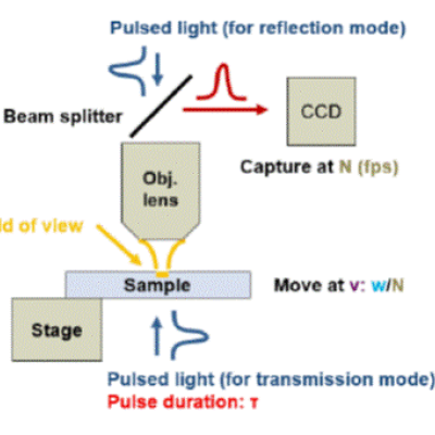
LLNL’s novel approach is to use a continuous moving camera with a scan speed of >1 mm/sec and a frame rate of 100 frames per second. The key is to have a light source that flashes with a duration of one nanosecond, thus essentially freezing the image with no blur. Clear images of high resolution can then be captured through a high-magnification objective lens (reflection mode)…
Image

CSP-POST provides the capability to inspect all incoming and outgoing emails while providing after-the-fact forensic capabilities. Using commercially available lightweight and serverless technologies, CSP-POST easily collects all email and parses it into easily searchable metadata, enriched and ready for analysis. The web-based application is deployed in a repeatable, testable, and auditable…
Image

U.S. Patent No. 11,555,965 describes LLNL’s invention of “Illumination Frustums” for photoconductive switches to capture and “frustrate” the light from leaving the frustum. LLNL researcher’s latest novel invention, “Twister Oven”, achieves this by encouraging laser light absorption in a photo conductor material. Light enters the oven twisting and reflecting, making near normal…
Image

For cooling a high power device, the novel approach is to use a thermoelectric cooler (TEC)-based embedded substrate with proper selection of the TEC material as an active cooler. The packaging configuration of TEC allows cooling the entire die without the use of a fluid. The process is compatible with the thin film TEC material. Standard semiconductor processes can be used…
Image

LLNL has invented a new system that uses public key cryptography to differentiate between human-generated text and AI-generated text. This invention can be used to validate that text is likely to be human generated for the purposes of sorting or gatekeeping on the internet, can detect cheating on essay assignments, and can be used as an automatic captcha that does away with the hassle of…
Image
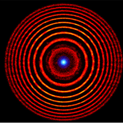
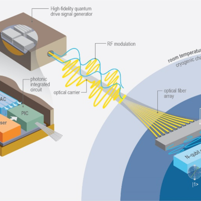
LLNL’s approach to the development of a wide-field, three-dimensional quantum (3DQ) microscope is to harness quantum entangled photons to form simultaneous 3D optical images, which could be a new paradigm for 3D volumetric imaging of biological specimens. The 3DQ microscope is comprised of a novel optical system with highly sensitive detectors and an on-demand light source of entangled…
Image

LLNL researchers faced this challenge by bridging the gap between VEDs and solid-state electronics (SSE). Their approach was to create a hybrid vacuum microelectronic device (VMD) architecture that combines the properties of vacuum as the electronic medium and the compact form factor and manufacturing scalability of semiconductor microelectronic chips.
Image

For this method, a Silicon on Insulator (SOI) wafer is used to tailor etch rates and thickness in initial steps of the process. The simple three step process approach is comprised of grayscale lithography, deep reactive-ion etch (DRIE) and liftoff of the SOI wafer. The liftoff process is used to dissolve the insulating layer, thus separating sections of the wafer as individual…
Image
LLNL’s novel approach combines 2-color spectroscopy with CRDS, a combination not previously utilized.
Image

The approach is to use Charge Balance Layers (CBLs) to create a superjunction device in wide bandgap materials. These CBLs enable the device to effectively spread the electric field over 2- or 3-dimensions within a semiconductor voltage sustaining layer instead of 1-dimension, thereby increasing the maximum voltage a device is capable of withstanding. The challenge of using CBLs is…
Image
This invention discloses a method to minimize transient variations in the wavelength- and/or pointing-behavior of an optic, without requiring a reduction in its thermal resistance, optical absorption, or operating irradiance. The invention employs a combination of a time-varying heat source and time-varying thermal resistance and/or heat sink temperature to achieve temperature stability of the…
Image
The approach is to build a high voltage insulator consisting of two materials: Poly-Ether-Ether-Ketone (“PEEK”) and Machinable Ceramic (“MACOR”). PEEK has a high stress tolerance but cannot withstand high temperatures, while MACOR has high heat tolerance but is difficult to machine and can be brittle. MACOR is used for the plasma-facing surface, while PEEK will handle the…
Image
This novel method of producing waveplates from isotropic optical materials (e.g. fused silica) consists of forming a void-dash metasurface using the following process steps:
Image

Design and construction of a photoconductive switch requires a diamond photoconductor illuminated by light of a certain excitation wavelength. The diamond material is specifically doped with substitutional nitrogen, which act as a source of electrons. The device architecture allows maximum light entering the aperture. The top and bottom electrodes are made of ultra wide band…
Image

The approach is to use a custom-designed frustrum and attach it to the optical fiber that connects to the PCSS. Light from the fiber enters the frustrum, spreads out, and enters the PCSS. Any unabsorbed light re-enters the frustrum and, because of its geometry, reflects back into the PCSS itself with only a negligible fraction escaping from the fiber. The shape of the novel…
Image
This invention concerns a new type of optic: a transient gas or plasma volume grating produced indirectly by small secondary lasers or directly by nonlinear processes using the primary beams themselves. When used in conjunction with advantageously placed shielding it offers a means of protecting the final optical components of a high-repetition-rate IFE facility. These transmission optics are…
Image
This invention utilizes transmission gratings to combine lasers of the same wavelength into a single collinear output. The transmission grating can be an all-bulk structure fabricated in fused silica, silicon, diamond, silicon nitride, etc. The transmission grating can also have dielectric coatings to increase diffraction efficiency and optical bandwidth. This invention makes possible…
Image
LLNL researchers in the NIF Directorate DoD Technologies RF Photonics Group explored phase modulation solutions to this signal processing challenge. Optical frequency combs offer phase noise characteristics that are orders of magnitude lower than available from commercial microwave references. The Photonics Group researchers recognized that by converting the intensity information into phase,…
Image

Lawrence Livermore National Laboratory (LLNL) is offering the opportunity to collaborate in accelerating artificial intelligence (AI) for applied science, including research in key areas such as advanced material design, 3D printing, predictive biology, energy systems, “self-driving” lasers and fusion energy research.
Image
CRETIN is a 1D, 2D, and 3D non-local thermodynamic equilibrium (NLTE) atomic kinetics/radiation transport code which follows the time evolution of atomic populations and photon distributions as radiation interacts with a plasma consisting of an arbitrary mix of elements. It can provide detailed spectra for comparing with experimental diagnostics.
Image
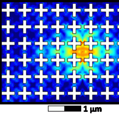
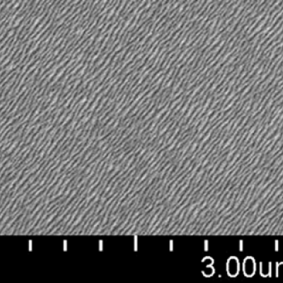
LLNL has developed a method of extending device lifetimes by imprinting into the device a shape that excludes specific vibrational modes, otherwise known as a phononic bandgap. Eliminating these modes prevents one of the primary energy loss pathways in these devices. LLNL’s new method enhances the coherence of superconducting circuits by introducing a phononic bandgap around the system’s…
Image
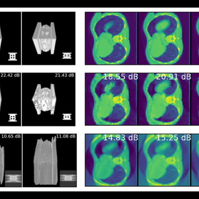
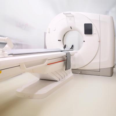
To solve these challenges using new and existing CT system designs, LLNL has developed an innovative software package for CT data processing and reconstruction. Livermore Tomography Tools (LTT) is a modern integrated software package that includes all aspects of CT modeling, simulation, reconstruction, and analysis algorithms based on the latest research in the field. LTT contains the most…
Image
Clinical images have a wealth of data that are currently untapped by physicians and machine learning (ML) methods alike. Most ML methods require more data than is available to sufficiently train them. In order to obtain all data contained in a clinical image, it is imperative to be able to utilize multimodal, or various types of, data such as tags or identifications, especially where spatial…
Image

Some COVID-19 diagnoses are utilizing computed tomography (CT)-scans for triage. CT-scans produce immediate results with high sensitivity. The digital images produced by a CT-scan require physicians to identify objects within the image to determine the presence of disease. Object identification can be done using machine learning (ML) techniques such as deep learning (DL) to improve speed and…
Image
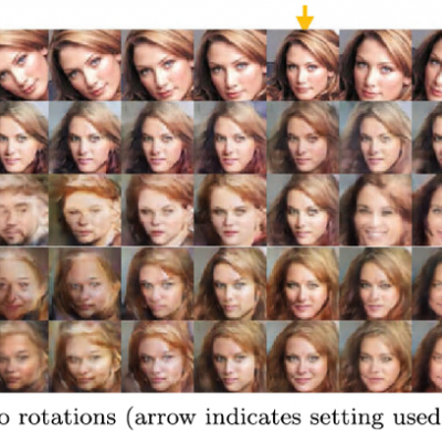
MimicGAN represents a new generation of methods that can “self-correct” for unseen corruptions in the data out in the field. This is particularly useful for systems that need to be deployed autonomously without needing constant intervention such as Automated Driver Assistance Systems. MimicGAN achieves this by treating every test sample as “corrupt” by default. The goal is to determine (a) the…
Image

Livermore Lab researchers have developed two new methods for improving the efficiency of laser drilling. The first method is based on multi-pulse laser technology. Two synchronized free-running laser pulses from a tandem-head Nd:YAG laser and a gated CW laser are capable of drilling through 1/8-in-thick stainless-steel targets at a standoff distance of 1 m without gas-assist. The combination of a…
Image

Livermore Lab's SBC grating optics benefit from the combination of the following key technologies:
- LLNL proprietary optical coating designs utilizing >100 thin film layers – enables ultra-low-loss, ppm transmission levels through the coating, high diffraction efficiency, and large bandwidth.
- LLNL proprietary dispersive surface relief structure…
Image
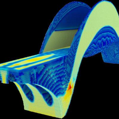
The LiDO code combines finite element analysis, design sensitivity analysis and nonlinear programming in a High-Performance Computing (HPC) environment that enables the solution of large-scale structural optimization problems in a computationally efficient manner. Currently, the code uses topology optimization strategies in which a given material is optimally distributed throughout the domain…
Image
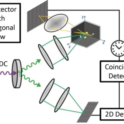
LLNL's 3D X-ray imager combines two different hardware pieces. The first is an x-ray optic with a depth-of-field that is small compared to the object under investigation. Reflective Wolter type x-ray optics are one such design. These hollow optics have a relatively large collection efficiency and can be designed with a large field of view. The depth of focus, which is the distance over which a…
Image

LLNL researchers have designed and tested performance characteristics for a multichannel pyrometer that works in the NIR from 1200 to 2000 nm. A single datapoint without averaging can be acquired in 14 microseconds (sampling rate of 70,000/s). In conjunction with a diamond anvil cell, the system still works down to about 830K.
Image

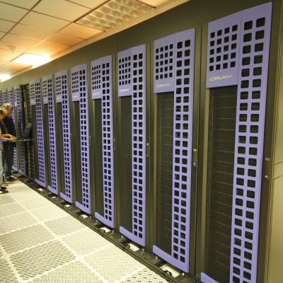
LLNL has developed a new method for securely processing protected data on HPC systems with minimal impact on the existing HPC operations and execution environment. It can be used with no alterations to traditional HPC operations and can be managed locally. It is fully compatible with traditional (unencrypted) processing and can run other jobs, unencrypted or not, on the cluster simultaneously…
Image

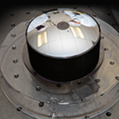
Monolithic Telescopes are a novel implementation of a solid catadioptric design form, instantiated in a monolithic block of fused silica.
Image
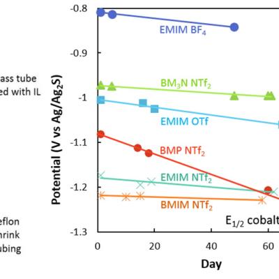
LLNL has developed a reference electrode that is a great improvement on the widely used silver or platinum wire QRE commonly used in electrochemistry in ionic liquids. This new reference electrode, based on a silver-sulfide coated silver wire, exhibits greatly improved stability over a QRE. The stability of our RE approaches that of the Ag/Ag+ RE, but unlike the Ag/Ag+ RE, the RE reported here…
Image
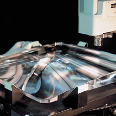
The LLNL method for optimizing as built optical designs uses insights from perturbed optical system theory and reformulates perturbation of optical performance in terms of double Zernikes, which can be calculated analytically rather than by tracing thousands of rays. A new theory of compensation is enabled by the use of double Zernikes which allows the performance degradation of a perturbed…
Image
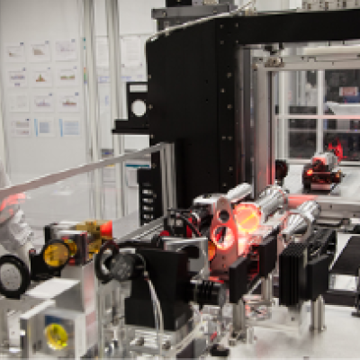
LLNL's method of equivalent time sampling incorporates an embedded system that generates the pulses used to trigger the external circuit and the data acquisition (DAQ). This removes the external reference clock, allowing the overall system clock rate to change based on the ability of the embedded system. The time delays needed to create the time stepping for equivalent time sampling is done by…
Image
LLNL has developed a new active memory data reorganization engine. In the simplest case, data can be reorganized within the memory system to present a new view of the data. The new view may be a subset or a rearrangement of the original data. As an example, an array of structures might be more efficiently accessed by a CPU as a structure of arrays. Active memory can assemble an alternative…
Image
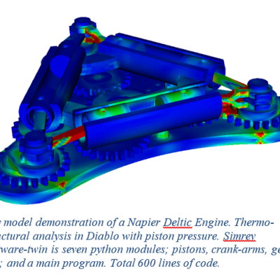
Simrev is a python library imported into a user-generated program. As the program grows in capability and complexity, the engineered product matures. The "software twin" handles all changes to product configuration and is the portal to running supercomputing analysis and managing workflow for engineering simulation codes. Assemblies become program modules; parts, materials, boundary conditions…
Image

LLNL researchers have developed a custom resin formulation which uses a dispersing solvent and only a multifunctional monomer as the binding agent. The dispersing solvent system typically used has multiple components meant to achieve excellent dispersal of silica in order to create a flowable resin (rather than a paste). The dispersing agent has low vapor pressure, which allows the 3D printed…
Image

LLNL’s Optically-based Interstory Drift Meter System provides a means to accurately measure the dynamic interstory drift of a vibrating building (or other structure) during earthquake shaking. This technology addresses many of the shortcomings associated with traditional strong motion accelerometer based building monitoring.
LLNL’s discrete diode position sensitive device is a newly…
Image
LLNL has developed a new system, called the Segmentation Ensembles System, that provides a simple and general way to fuse high-level and low-level information and leads to a substantial increase in overall performance of digital image analysis. LLNL researchers have demonstrated the effectiveness of the approach on applications ranging from automatic threat detection for airport security, to…
Image
The selected industrial partner and LLNL will enter into a Cooperative Research and Development Agreement (CRADA) to develop the next generation of laser technologies for MEGa-ray systems and to create a next generation of MEGa-ray sources that could be marketed to both the industrial and academic communities.
The MEGa-ray system developed will be based on LLNL's proprietary, multi-…
Image

The Optical Transconductance Varistor (OTV, formerly Opticondistor) overcomes depletion region voltage limitations by optically exciting wide bandgap materials in a compact package. A 100μm thick crystal could have the capability approaching 40kV and would replace numerous equivalent junction devices. Thus, unlike present junction transistors or diodes, this wide bandgap device can be stacked…
Image

The new LLNL technique works by transiently removing and trapping concrete or rock surface material, so that contaminants are confined in a manner that is easy to isolate and remove. Our studies suggest that 10 m2 of surface could be processed per hour. The technique easily scales to more surface/hr.
Image
LLNL's Slurry Stabilization Method provides a chemical means of stabilizing a polishing compound in suspension at working concentrations without reducing the rate of material removal. The treated product remains stable for many months in storage.
Image
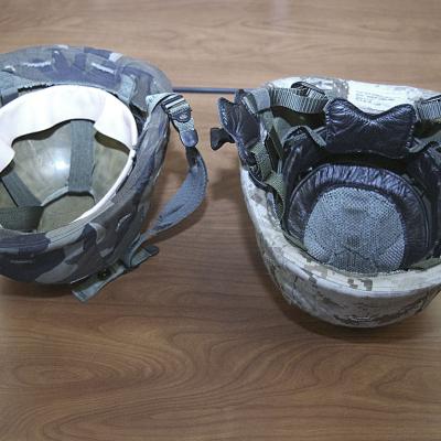
LLNL's high fidelity hydrocode is capable of predicting blast loads and directly coupling those loads to structures to predict a mechanical response. By combining this code and our expertise in modeling blast-structure interaction and damage, along with our access to experimental data and testing facilities, we can contribute to the design of protective equipment that can better mitigate the…
Image
The technology that is available has the capability to inject realistic radiation detection spectra into the amplifier of a radiation detector and produce the all the observables that are available with that radiation detection instrument; count-rate, spectrum, dose rate, etc.
The system uses the capability of LLNL to generate the source output for virtually any source and determine…
Image
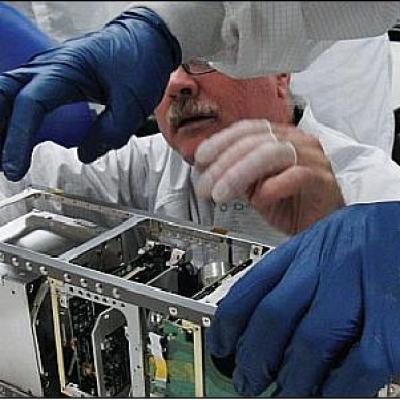
LLNL is developing the Space-based Telescopes for Actionable Refinement of Ephemeris (STARE). STARE is a constellation of low cost nano-satellites (less than 5Kg) in low-earth orbit dedicated to the observation of space debris in conjunction with a ground-based infrastructure for maintenance, coordination and data processing. Each nano-satellite in the constellation is capable of recording an…