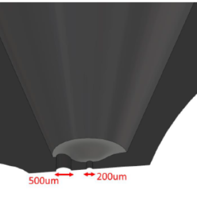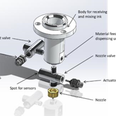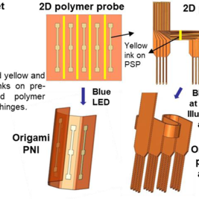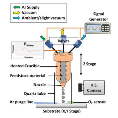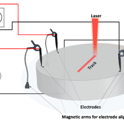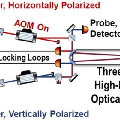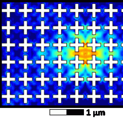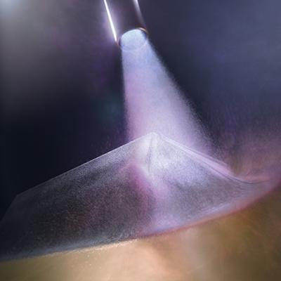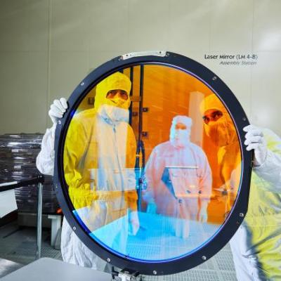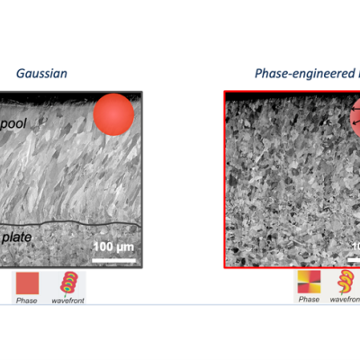
LLNL researchers have developed a novel system that can shape the profile of the laser beam during printing or welding. The phase engineered approach in beam shaping enables in situ process control of its energy distribution at melt-relevant timescales.
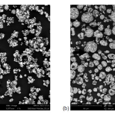
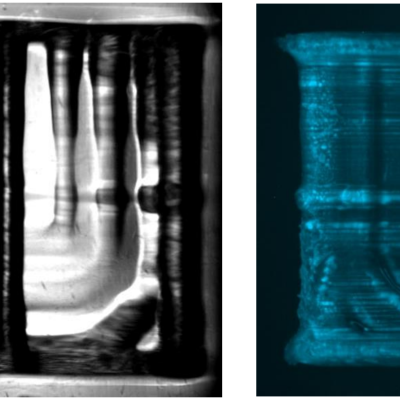
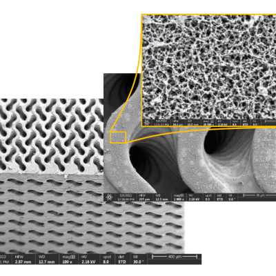
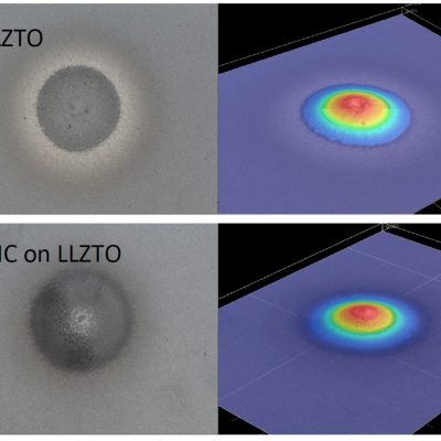
Image Caption: SS 316L L-PBF melt pool engineered with LLNL beam shaping demonstrate control of microstructure grain refinement (…